Camera-LCD Interfacing with Microcontroller (alec green)
 . introduction

CAMERA
 . interpreting vsync/href
 . interpreting pixel values
 . fifo frame buffer
 . sccb/i2c communication

LCD
 . populating with pixels

 . references
![]() Transfer of pixels from camera to LCD is a crucial element of this application.
Transfer of pixels from camera to LCD is a crucial element of this application.
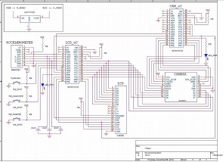
In order to transfer pixels from the camera to the LCD at an 'acceptable' frame rate, a shared 'pixel bus' was created in which a uC, LCD, and camera are all connected together. This allows image pixels to be directly transferred from camera to LCD without being unnecessarily passed through the uC, while at the same time allowing a uC to write pixels to or read pixels from the LCD as desired (eg write to overlay graphics, read to perform image processing operations on pixels). Further, this configuration allows the uC to randomly access pixels from the LCD, which is necessary for image processing algorithms that perform local operations. This is much appreciated, as the camera's FIFO buffer is sequential access and thus does not allow memory reads from arbitrary locations.
Initially, a bit-banged clock was used to transfer the pixels from camera frame buffer to LCD, providing a framerate of 7.5Hz. However, a selectively enabled PWM operating at its maximum frequency of 12MHz was then used as a more autonomous clocking signal. A pulse accumulator is tied to the PWM signal in order to stop the PWM when the appropriate number of pixels have been transferred. A quick calculation shows that the PWM can transfer an entire 'QVGA' frame (313x240) of 2B pixels at $ (313*240*2) / 12MHz = 12.5ms $. This updates the LCD at the 30Hz framerate output by the camera. ..(this nears the human visual system's temporal resolution).. However, it's clear that this could allow >60Hz framerate if desired.
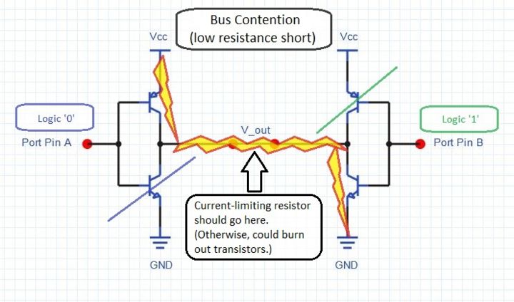
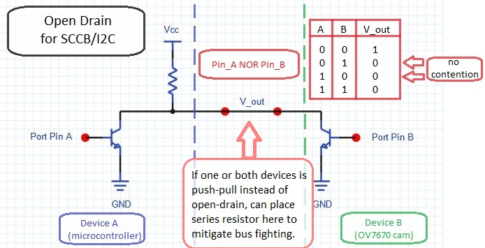
To avoid bus contention over the shared pixel bus and WRITE signal bus, software 'locks' are used to control when relevant uC, LCD, and camera push-pull pins are allowed to be configured as outputs.
picture of push-pull output w/ output buffers
References
[]
[]
[]
[]
